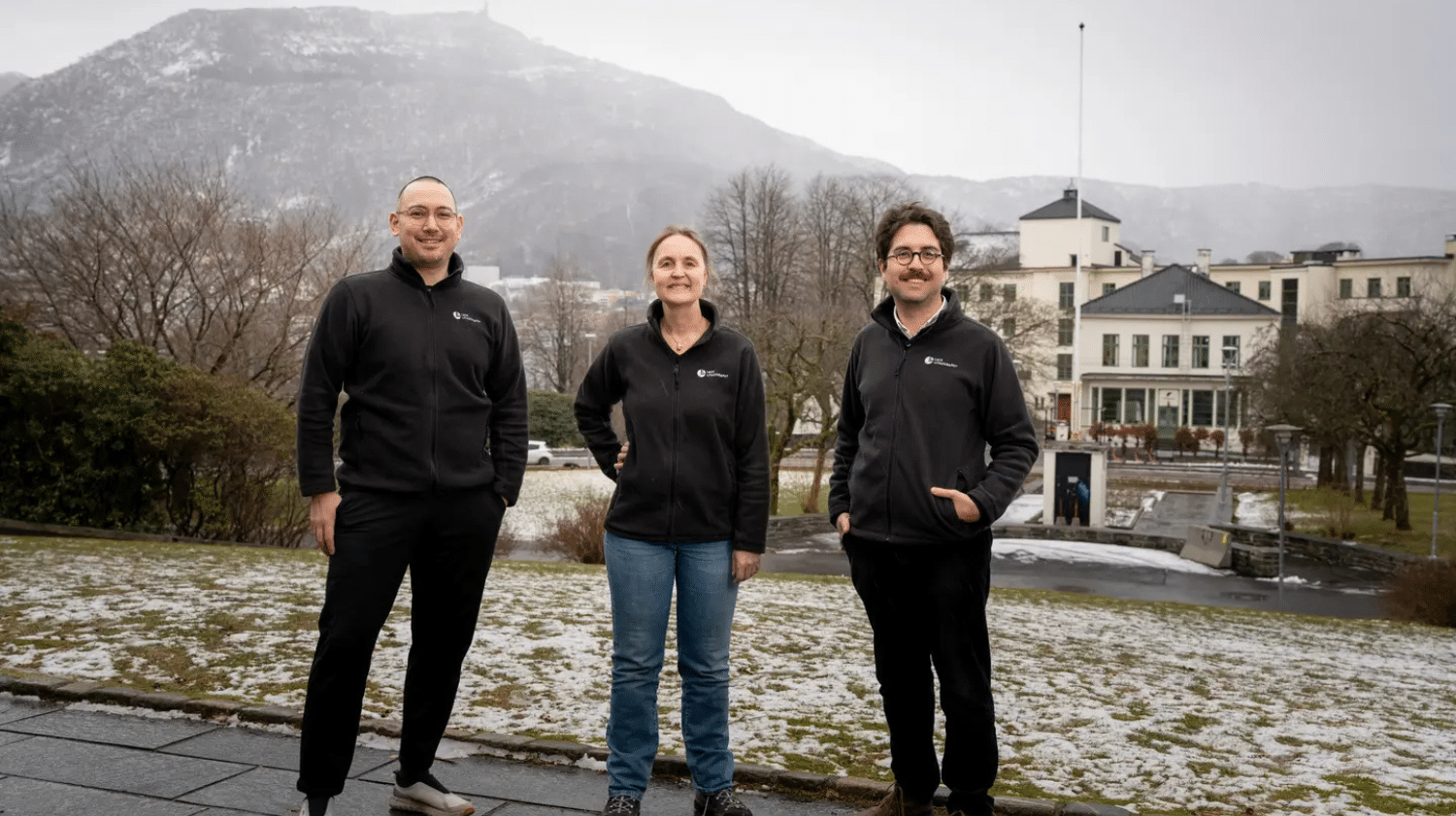
Lace Lithography, a semiconductor equipment startup, has raised €34.5 million in a Series A round led by Atomico, with participation from M12 (Microsoft’s venture fund), Linse Capital, SETT, and Nysnø, alongside existing investors Vsquared Ventures, Future Ventures, and Runa Capital.
Founded in 2023, the company has now secured over €51.7 million in total funding. The investment will support the development of next-generation lithography systems aimed at extending the limits of semiconductor performance.
What The Company Does
Lace Lithography is developing a new class of chip fabrication technology based on atom lithography, specifically using metastable helium atoms instead of light to pattern semiconductor wafers. This approach, referred to as Beyond-EUV (BEUV), is designed to overcome the physical limitations of existing extreme ultraviolet (EUV) lithography systems.
Traditional lithography relies on photons, which are constrained by diffraction limits that restrict how small features on chips can be made. By replacing light with atoms, Lace aims to achieve significantly higher resolution, potentially enabling features up to ten times smaller than those produced by current leading systems.
In addition to improved precision, the company’s technology is designed to reduce energy consumption, system complexity, and overall costs. Lace is also positioning its solution as compatible with existing semiconductor foundry infrastructure, allowing integration without major operational changes.
Market Context / Industry Background
The semiconductor industry is facing increasing challenges as it approaches the physical and economic limits of current manufacturing technologies. Advanced lithography systems have become significantly more expensive and complex, with leading machines costing hundreds of millions of euros per unit and requiring highly specialized supply chains.
At the same time, demand for computing power continues to grow, driven by artificial intelligence, data processing, and high-performance applications. This creates pressure on chip manufacturers to deliver smaller, more efficient, and more powerful semiconductors.
The concentration of advanced lithography capabilities among a limited number of suppliers has also introduced structural bottlenecks in the global semiconductor ecosystem. As a result, alternative approaches that can extend Moore’s Law and diversify technological pathways are attracting increased attention from investors and industry stakeholders.
Founder / Investor Commentary
CEO and co-founder Dr. Bodil Holst emphasized that current lithography methods are reaching their limits as computing demands accelerate. She described Lace’s approach as a fundamentally new pathway that enhances existing manufacturing processes rather than replacing them, with the goal of enabling continued progress in chip performance.
From an investor perspective, Atomico highlighted the growing strain on semiconductor production, noting that the rising cost, energy requirements, and complexity of current systems are creating a bottleneck at a critical moment for global compute demand. The firm pointed out that while the industry has long anticipated these challenges, viable alternatives have remained limited until now.
Growth Plans / Use Of Funds
The Series A funding will be used to further develop Lace Lithography’s BEUV systems and advance them toward industrial-scale deployment. This includes continued research and engineering, as well as efforts to validate the technology within semiconductor manufacturing environments.
The company is expected to focus on scaling its platform to meet the requirements of commercial foundries, while strengthening partnerships within the semiconductor ecosystem. As development progresses, Lace aims to position its technology as a complementary solution that enhances existing fabrication processes and extends their performance capabilities.
About Lace Lithography
Lace Lithography is a semiconductor equipment company developing atom-based lithography systems. Founded in 2023. Headquartered in Bergen, Norway. The company’s core mission is to enable the next generation of chip manufacturing by overcoming the physical limitations of light-based lithography and supporting continued advances in computing performance.
